| CPC H03K 17/08122 (2013.01) [H02H 3/093 (2013.01); H03K 2217/0036 (2013.01)] | 20 Claims |
|
1. A method, comprising:
disconnecting a power line providing current to a load having inductance, the disconnecting comprising:
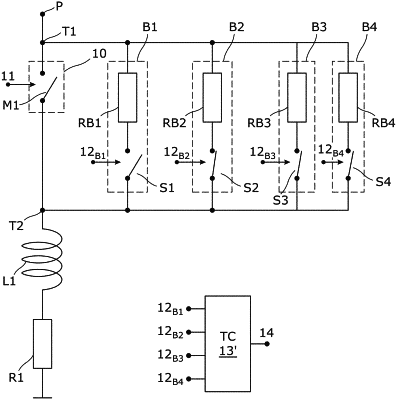
connecting a primary solid state or discrete solution switch arrangement between the power line and the load, the primary solid state or discrete solution switch arrangement operable by primary turn on or turn off control commands to assume a conductive or non-conductive state;
connecting, in parallel with the primary solid state or discrete solution switch arrangement, one or more protection branches each providing a respective low RC path comprising a series connected resistive element a secondary solid state or discrete solution switch that is operable by branch turn on or turn off control commands to assume a conductive or non-conductive state, and a capacitor between a gate of the secondary solid state or discrete solution switch and the load;
applying, to the primary solid state or discrete solution switch arrangement, a primary turn on control command effective to cause the primary solid state or discrete solution switch arrangement to assume the conductive state;
applying, to the secondary solid state or discrete solution switches, a secondary turn on control command effective to cause the secondary solid state or discrete solution switches to assume the conductive state;
detecting a short circuit in the load;
applying, responsive to detecting the short circuit in the load and to the primary solid state or discrete solution switch arrangement, a primary turn off control command effective to cause the primary solid state or discrete solution switch arrangement to assume the non-conductive state; and
applying, to the secondary solid state or discrete solution switch of the protection branches, a branch turn off control command that is delayed because of the respective low RC path at each of the protection branches by a predetermined time interval relative to when the primary turn off control command is applied to the primary solid state or discrete solution switch arrangement such that energy associated with the inductance dissipates through the series connected resistive elements while the secondary solid state or discrete solution switches assume the conductive state during the delay,
wherein the capacitors are configured to cause the secondary solid state or discrete solution switches of the protection branches to switch at respective predetermined speeds.
|