| CPC H03K 3/0375 (2013.01) [G06F 1/3237 (2013.01); H03K 3/0372 (2013.01); H03K 3/356086 (2013.01); H03K 19/0016 (2013.01)] | 20 Claims |

|
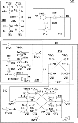
1. A circuit comprising:
a first power node configured to have a first voltage level;
a second power node configured to have a second voltage level different from the first voltage level;
a reference node configured to have a reference voltage level;
a master latch configured to output a first data bit based on a received data bit;
a slave latch comprising:
a first inverter configured to output a second data bit based on the first data bit; and
a second inverter configured to output an output data bit based on a selected one of the first data bit or a third data bit;
a first level shifter configured to output the third data bit based on a fourth data bit; and
a retention latch configured to output the fourth data bit based on the second data bit, wherein
each of the first and second inverters and the first level shifter is coupled between the first power node and the reference node, and
the retention latch comprises a plurality of transistors coupled between the second power node and the reference node.
|