| CPC H03K 3/0372 (2013.01) [G01R 31/3177 (2013.01); H03K 3/038 (2013.01); H03K 3/35625 (2013.01); H03K 19/20 (2013.01)] | 17 Claims |
|
1. An apparatus comprising:
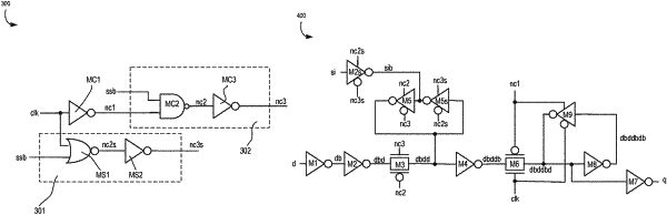
a latch that includes a data path and a scan path, wherein the latch includes:
a transmission gate coupled on the data path between a data input and a keeper node; and
a memory circuitry coupled to the keeper node, wherein the scan path is coupled to the memory circuitry, wherein the memory circuitry includes:
a first tri-statable inverter having an input coupled to the keeper node; and
a second tri-statable inverter having an input coupled to an output of the first tri-statable inverter and the scan path, wherein an output of the second tri-statable inverter is coupled to the keeper node; and
scan clock circuitry to generate scan clock signals for a scan mode of the latch, the scan clock circuitry comprising:
an inverter having an input and an output, wherein an input of the inverter is to receive an input clock;
an AND logic coupled to the output of the inverter, wherein the AND logic is to receive a scan select signal; and
an OR logic coupled to the input of the inverter, wherein the OR logic is to receive the scan select signal.
|