| CPC H03F 1/0216 (2013.01) [H03F 1/32 (2013.01); H03F 3/19 (2013.01); H03F 1/0211 (2013.01); H03F 1/0244 (2013.01); H03F 2200/165 (2013.01); H03F 2200/451 (2013.01)] | 11 Claims |
|
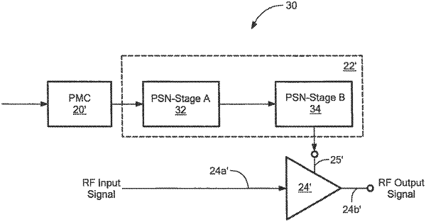
1. A multi-stage pulse shaping network configured to be coupled to a bias terminal of a radio frequency (RF) amplifier and configured for use in a discrete supply modulation system, the multi-stage pulse shaping network comprising:
(a) a first pulse shaping network (PSN) stage having an input configured to be coupled to a power management circuit (PMC) and having an output;
(b) one or more second PSN stages, each of the one or more second PSN stages physically spaced apart and distant from the first PSN stage and each of the second PSN stages having an input configured to be coupled to the output of the first PSN stage and having an output configured to be coupled to a bias terminal of an RF amplifier; and
(c) a signal path having a first end coupled to the output of the first PSN stage and having a second end coupled to the inputs of the one or more second PSN stages,
wherein the first PSN stage together with the one or more second PSN stages are configured to filter signals resultant from transitions between discrete voltage levels received from the PMC.
|