| CPC H03B 5/32 (2013.01) [H03H 9/0552 (2013.01); H03H 9/1014 (2013.01)] | 7 Claims |
|
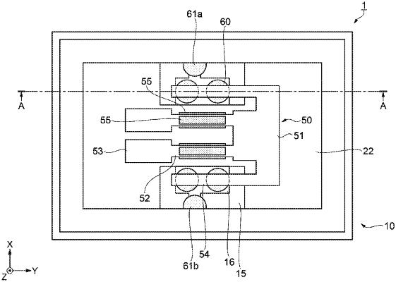
1. An oscillator comprising:
a resonator element;
a circuit element that is coupled to the resonator element and is configured to output a clock signal; and
a container that houses the resonator element and the circuit element and includes a substrate mounted with the circuit element,
wherein the circuit element includes a plurality of terminals including
a first coupling terminal coupled to the resonator element,
a second coupling terminal coupled to the resonator element and disposed side by side with the first coupling terminal in a first direction, and
an output terminal that is disposed adjacent to the first coupling terminal in a second direction orthogonal to the first direction and from which the clock signal is output,
wherein the substrate includes
a first layer including a first surface mounted with the circuit element and a second surface in a front and back relationship with the first surface,
a second layer stacked on the first layer,
a first coupling electrode provided on the first surface and coupled to the first coupling terminal,
a second coupling electrode provided on the first surface and coupled to the second coupling terminal,
an output electrode provided on the first surface and coupled to the output terminal,
a first coupling wiring provided on the second surface and coupled to the first coupling electrode,
a second coupling wiring provided on the second surface and coupled to the second coupling electrode,
an output wiring provided on the second surface and coupled to the output electrode, and
a shield wiring that is provided between the first coupling wiring and the output wiring on the second surface and to which a direct-current potential is applied.
|