| CPC H02M 3/07 (2013.01) [H03L 7/0891 (2013.01); H04L 7/033 (2013.01)] | 19 Claims |
|
1. A clock data recovery circuit comprising:
an input configured to receive a data signal;
a voltage controlled oscillator comprising a clock;
a phase detector configured to generate an early signal and a late signal, which are indicative of whether a phase of the clock of the voltage controlled oscillator is early or late relative to a phase of the data signal; and
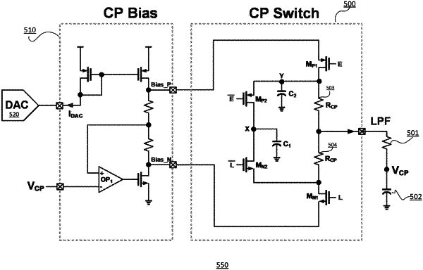
a charge pump comprising
a first switch responsive to the early signal,
a second switch responsive to the late signal,
a pair of resistive elements connected in series between a drain of the first switch and a drain of the second switch to reduce glitch current at an output of the charge pump during transitions of the early signal and the late signal between high and low states, the pair of resistive elements configured to provide resistance between an output of the charge pump and the first switch and the second switch and to drive the voltage controlled oscillator, and
a capacitor connected to the drain of the first switch and to a first resistive element of the pair of resistive elements, the first resistive element limiting an amount of charge flow from the output of the charge pump back through the first resistive element to the capacitor.
|