| CPC H02M 1/008 (2021.05) [H02M 1/0025 (2021.05); H02M 3/156 (2013.01); H02M 3/157 (2013.01); H02M 3/158 (2013.01)] | 24 Claims |

|
1. A first circuit, comprising:
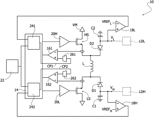
at least one pair of output nodes, the pair of output nodes comprising a first output node and a second output node with an inductor arranged intermediate therebetween;
current drive circuitry comprising a first switch and a second switch coupled to opposed ends of the inductor, the first switch and the second switch switchable between a non-conductive state and a conductive state to control current flow through the inductor and produce a first output voltage at the first output node and a second output voltage at the second output node;
current sensing circuitry sensitive to a current intensity through the inductor and configured to compare the current intensity sensed with at least one reference value; and
switching control circuitry coupled with the first switch and the second switch, with the first output node and the second output node, and with the current sensing circuitry, wherein the switching control circuitry comprises a timer circuit configured to produce a timing signal with a timing frequency, and wherein the switching control circuitry is configured to:
control a switching frequency of the first switch and the second switch between the non-conductive state and the conductive state as a function of the first output voltage at the first output node, the second output voltage at the second output node, and a result of comparing the current intensity sensed with the at least one reference value;
compare a value of the switching frequency with the timing frequency to produce a frequency error value;
generate an integrated frequency error value by integrating the frequency error value; and
produce the at least one reference value as a function of the integrated frequency error value to maintain a constant value for the switching frequency.
|