| CPC H01S 5/4043 (2013.01) [H01S 5/125 (2013.01); H01S 5/2036 (2013.01); H01S 5/3095 (2013.01)] | 20 Claims |
|
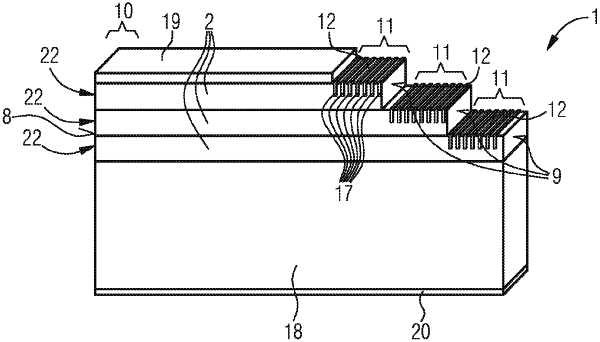
1. An edge emitting semiconductor laser comprising
first and second laser diodes, each of which is configured to generate electromagnetic radiation, wherein
the first and second laser diodes are arranged one above another in a vertical direction,
the first and second laser diodes are monolithically connected to one another,
one or a plurality of frequency-stabilizing element are arranged in an end region of the first and second laser diodes, wherein the second laser diode regionally is not covered by the first laser diode arranged above the second laser diode in a vertical direction and has one of the frequency-stabilizing elements in the uncovered region, and
at least one of the first and second laser diodes comprises:
first and second cladding layers,
first and second propagation layers positioned between the first and second cladding layers, wherein vertical extents of a beam profile are based upon a refractive index of the first and second propagation layers, and
an active zone positioned between the first and second propagation layers.
|