| CPC H01P 5/107 (2013.01) [H01Q 1/2283 (2013.01); H01Q 1/3233 (2013.01); H05K 1/181 (2013.01); H05K 2201/037 (2013.01); H05K 2201/09985 (2020.08); H05K 2201/10098 (2013.01)] | 20 Claims |
|
1. A waveguide assembly comprising:
a printed circuit board (PCB) comprising:
at least one PCB layer that includes a first surface and a second surface positioned opposite and in parallel with the first surface;
a plated slot configured to channel an electromagnetic (EM) energy from a planar dimension in parallel with the first surface to a vertical dimension that is orthogonal to the planar dimension, the plated slot comprising an opening surrounded by a conductive material to enable electrical connections between the first surface and the second surface, the opening configured to transfer the EM energy between the first surface and the second surface; and
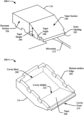
a waveguide cavity mounted directly on the first surface and positioned over the plated slot, the waveguide cavity being hollow and configured to perform impedance matching of the EM energy while guiding the EM energy from the first surface to the second surface via the plated slot, the waveguide cavity comprising:
a bottom surface configured to be open, the bottom surface mounted directly on the first surface of the PCB;
a taper section configured to taper a height of the waveguide cavity, the height of the waveguide cavity gradually increasing at a taper angle from a cavity front to a cavity middle, the height of the waveguide cavity being tapered to enable impedance matching of the EM energy; and
a resonant section connected to the taper section at the cavity middle, the resonant section being rectangular in shape.
|