| CPC H01L 33/62 (2013.01) [H01L 25/0753 (2013.01); H01L 33/005 (2013.01); H01L 33/38 (2013.01); H01L 33/54 (2013.01); H01L 2933/005 (2013.01); H01L 2933/0016 (2013.01); H01L 2933/0066 (2013.01)] | 8 Claims |
|
1. A method for manufacturing a multi-sided light-emitting circuit board, the method comprising the following steps:
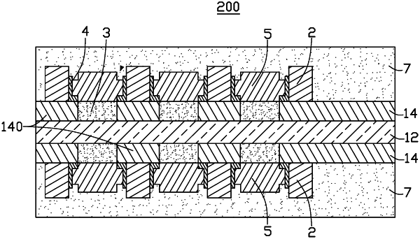
providing a copper-clad substrate, the copper-clad substrate comprising a transparent substrate layer and a first copper foil layer on at least one surface of the transparent substrate layer;
forming the first copper foil layer into a first conductive circuit layer, the first conductive circuit layer revealing a portion of the transparent substrate layer, and the first conductive circuit layer comprising a plurality of conductive portions arranged in an array;
forming a metal piece on each of the conductive portions, a size of each metal piece smaller than a size of the conductive portion connected to the metal piece, and adjacent metal pieces spaced apart to form an accommodation space;
forming a transparent glue layer on a surface of the transparent substrate layer and in spaces formed by the conductive portions, the glue layer flush with the first conductive circuit layer;
providing light-emitting chip, the light-emitting chip comprising two electrodes, the two electrodes respectively located at opposite ends of the light-emitting chip, and the light-emitting chip arranged in the accommodating space so that the two electrodes at the opposite ends of the light-emitting chip are electrically connected to two adjacent metal pieces; and
forming an encapsulant layer on a surface of the first conductive circuit layer, the encapsulant layer encapsulating the metal pieces and the light-emitting chips;
wherein after the glue layer is formed and before mounting the light-emitting chip to sidewalls of every two adjacent metal pieces, the method further comprises:
forming a conductive paste on each of the conductive portions, the conductive paste surrounding a sidewall of the metal piece connected to the conductive portion; and
after the light-emitting chip is mounted on the sidewalls of each two adjacent metal pieces, performing a reflow soldering step, so that the light-emitting chip and the conductive paste are electrically connected.
|