| CPC H01L 33/58 (2013.01) [C03B 19/066 (2013.01); C03C 3/06 (2013.01); C03C 4/0085 (2013.01); H01L 25/0753 (2013.01); H01L 33/486 (2013.01); C03B 2201/04 (2013.01); C03C 2201/23 (2013.01); H01L 33/32 (2013.01); H01L 2933/0058 (2013.01)] | 16 Claims |
|
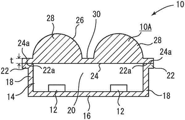
1. A silica glass member for hermetic sealing of an ultraviolet SMD LED element that is configured to emit light in a wavelength range of from 250 nm to 350 nm and is placed in a hermetic sealing container having a container outer periphery joining plain surface formed in an outer peripheral portion thereof, the silica glass member for hermetic sealing comprising:
a silica glass substrate, which is homogeneously and integrally formed without an internal boundary, wherein the silica glass substrate has:
a first surface on an inside opposed to the SMD LED element; and
a second surface on an outside corresponding to the first surface, wherein an outer peripheral portion of the first surface has formed therein a substrate joining plain surface for joining to the container outer periphery joining plain surface, and the second surface on the outside corresponding to the first surface has formed therein a lens convex portion configured to process emitted light from the ultraviolet SMD LED element, wherein the substrate joining plain surface formed in the first surface has a surface accuracy equal to 1 μm or less and a surface roughness of 0.05 μm to 0.3 μm in terms of Ra value, and the lens convex portion in the second surface has a surface roughness of 0.05 μm to 0.5 μm in terms of Ra value.
|