US 11,757,055 B2
Electromagnetic wave detector, and electromagnetic wave detector array
Shoichiro Fukushima, Tokyo (JP); Masaaki Shimatani, Tokyo (JP); and Shimpei Ogawa, Tokyo (JP)
Assigned to MITSUBISHI ELECTRIC CORPORATION, Tokyo (JP)
Appl. No. 16/980,437
Filed by Mitsubishi Electric Corporation, Tokyo (JP)
PCT Filed Feb. 28, 2019, PCT No. PCT/JP2019/007781
§ 371(c)(1), (2) Date Sep. 14, 2020,
PCT Pub. No. WO2020/003613, PCT Pub. Date Jan. 2, 2020.
Claims priority of application No. 2018-121156 (JP), filed on Jun. 26, 2018.
Prior Publication US 2021/0020797 A1, Jan. 21, 2021
Int. Cl. H01L 31/032 (2006.01); G01J 1/02 (2006.01); H01L 31/0384 (2006.01)
CPC H01L 31/032 (2013.01) [G01J 1/0295 (2013.01); H01L 31/0384 (2013.01)] 17 Claims
OG exemplary drawing
 
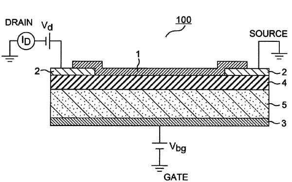
1. An electromagnetic wave detector comprising:
an insulating layer formed of a rare earth oxide;
a pair of electrodes provided on the insulating layer so as to be arranged to face each other across a gap; and
a two-dimensional material layer provided on the insulating layer so as to be electrically connected to the pair of electrodes, wherein
the rare earth oxide contains a base material made of an oxide of a first rare earth element, and a second rare earth element different from the first rare earth element, which is activated in the base material.