| CPC H01L 29/78696 (2013.01) [H01L 29/401 (2013.01); H01L 29/41733 (2013.01); H01L 29/41775 (2013.01); H01L 29/42364 (2013.01); H01L 29/42384 (2013.01); H01L 29/66742 (2013.01); H01L 29/7869 (2013.01); H01L 29/78618 (2013.01)] | 20 Claims |
|
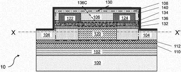
1. A semiconductor structure comprising:
a first dielectric layer;
a gate electrode embedded within the first dielectric layer;
a gate dielectric layer;
a channel layer comprising a semiconducting metal oxide material;
a second dielectric layer; and
a source electrode and a drain electrode embedded in the second dielectric layer and contacting a respective portion of a top surface of the channel layer,
wherein:
a combination of the gate electrode, the gate dielectric layer, the channel layer, the source electrode, and the drain electrode form a transistor;
a total length of a periphery of a bottom surface of the channel layer that overlies the gate electrode is greater than or equal to a width of the gate electrode;
the first dielectric layer comprises a top horizontal surface that contacts the gate dielectric layer and a recessed horizontal surface that does not underlie the gate dielectric layer; and
a set of sidewall segments of the first dielectric layer adjoins the top horizontal surface of the first dielectric layer to the recessed horizontal surface of the first dielectric layer.
|