| CPC H01L 29/7827 (2013.01) [H01L 29/41741 (2013.01); H01L 29/41766 (2013.01); H01L 29/6653 (2013.01); H01L 29/66666 (2013.01)] | 14 Claims |
|
1. A vertical transport field effect transistor (VTFET) device comprising:
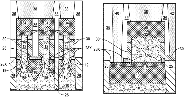
at least one semiconductor fin extending upward from a surface of a substrate and located in a first active device region, wherein a trench isolation structure is located in the substrate and at an edge of the first active device region;
a bottom source/drain region located beneath, and on each side of, the at least one semiconductor fin;
a moon-shaped bottom spacer located laterally adjacent to a lower portion of at least a first side of the at least one semiconductor fin and above the bottom source/drain region, wherein the moon-shaped bottom spacer has a convex upper surface and a planar bottommost surface;
a functional gate structure contacting a middle portion of the at least one semiconductor fin and located on the convex upper surface of the moon-shaped bottom spacer;
a top spacer contacting an upper portion of the at least one semiconductor fin and on a surface of the functional gate structure; and
a top source/drain region contacting an upper surface of the at least one semiconductor fin.
|