| CPC H01L 29/78 (2013.01) [G11C 11/404 (2013.01); G11C 11/4097 (2013.01); G11C 16/02 (2013.01); H01L 23/5226 (2013.01); H01L 23/5283 (2013.01); H01L 29/7841 (2013.01); H10B 10/12 (2023.02); H10B 12/20 (2023.02); H10B 43/20 (2023.02); H10B 63/30 (2023.02); H10B 69/00 (2023.02); G11C 11/412 (2013.01); G11C 16/0483 (2013.01); G11C 2213/71 (2013.01)] | 20 Claims |
|
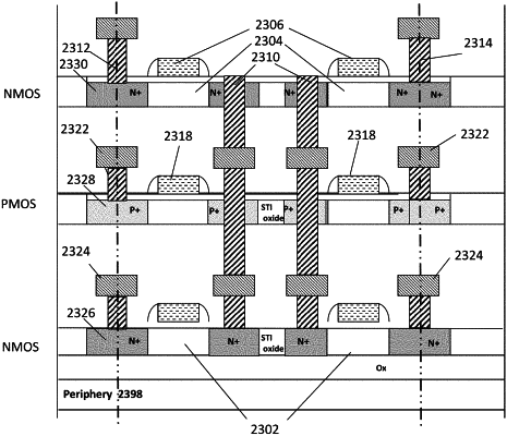
1. A semiconductor device, the device comprising:
a first silicon layer comprising first single crystal silicon;
an isolation layer disposed over said first silicon layer;
a first metal layer disposed over said isolation layer;
a second metal layer disposed over said first metal layer;
a first level comprising a plurality of transistors, said first level disposed over said second metal layer,
wherein said isolation layer comprises an oxide to oxide bond surface,
wherein said plurality of transistors comprise a second single crystal silicon region; and
a third metal layer disposed over said first level,
wherein a typical first thickness of said third metal layer is at least 50% greater than a typical second thickness of said second metal layer.
|