| CPC H01L 29/66363 (2013.01) [H01L 21/2652 (2013.01); H01L 29/7455 (2013.01)] | 17 Claims |
|
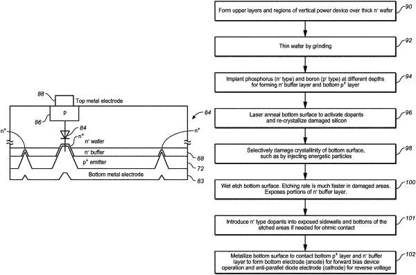
1. A method for forming a vertical power device comprising:
providing a silicon substrate wafer having a top surface and a bottom surface;
forming n-type and p-type device regions in the top surface of the wafer;
thinning the wafer from the bottom surface;
implanting dopants into the bottom surface such that the bottom surface is a first layer of a first conductivity type, wherein the first layer abuts a second layer, having a second conductivity type, overlying the first layer;
causing the bottom surface of the wafer to have a damaged crystalline structure so that the silicon will etch unevenly in an etching process;
etching the bottom surface, wherein areas of the bottom surface have non-uniform etch rates, until areas of the second layer are exposed; and
forming a first metal electrode on the bottom surface such that the first metal electrode directly contacts the first layer and the second layer, wherein contact with the second layer forms an anti-parallel diode, and wherein the first metal electrode conducts current in a forward direction when the device is on, and the first metal electrode conducts a reverse current when the device is off and a reverse voltage is applied across the device.
|