US 11,757,013 B2
Drain and/or gate interconnect and finger structure
Frank Trang, San Jose, CA (US); Zulhazmi Mokhti, Morgan Hill, CA (US); and Haedong Jang, San Jose, CA (US)
Assigned to Wolfspeed, Inc., Durham, NC (US)
Filed by Wolfspeed, Inc., Durham, NC (US)
Filed on Jun. 7, 2022, as Appl. No. 17/834,395.
Application 17/834,395 is a continuation of application No. 16/998,287, filed on Aug. 20, 2020, granted, now 11,424,333.
Application 16/998,287 is a continuation of application No. 16/375,398, filed on Apr. 4, 2019, granted, now 10,763,334.
Application 16/375,398 is a continuation in part of application No. 16/032,571, filed on Jul. 11, 2018, granted, now 10,483,352, issued on Nov. 19, 2019.
Prior Publication US 2022/0302272 A1, Sep. 22, 2022
This patent is subject to a terminal disclaimer.
Int. Cl. H01L 23/52 (2006.01); H01L 29/423 (2006.01); H01L 23/522 (2006.01); H01L 23/528 (2006.01); H01L 29/06 (2006.01); H01L 29/08 (2006.01); H01L 29/417 (2006.01); H01L 29/778 (2006.01); H01L 29/78 (2006.01)
CPC H01L 29/42316 (2013.01) [H01L 23/528 (2013.01); H01L 23/5226 (2013.01); H01L 29/0696 (2013.01); H01L 29/0847 (2013.01); H01L 29/41758 (2013.01); H01L 29/778 (2013.01); H01L 29/7816 (2013.01)] 20 Claims
OG exemplary drawing
 
1. A transistor device, comprising:
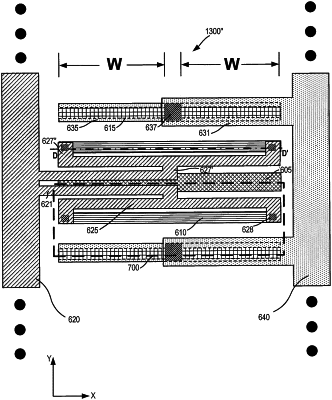
a semiconductor structure;
a drain finger extending on the semiconductor structure in a first direction;
a drain interconnect extending on the semiconductor structure in the first direction, the drain interconnect having a first end and a second end;
a first conductive via coupled between the drain interconnect and the drain finger; and
a second conductive via coupled to the drain interconnect at an interior position of the drain interconnect that is offset from the first and second ends of the drain interconnect,
wherein the second conductive via connects to an upper side of the drain interconnect and the first conductive via connects to a lower side of the drain interconnect.