| CPC H01L 29/36 (2013.01) [H01L 21/425 (2013.01); H01L 29/24 (2013.01); H01L 29/7813 (2013.01); H01L 29/8613 (2013.01); H01L 29/872 (2013.01)] | 4 Claims |
|
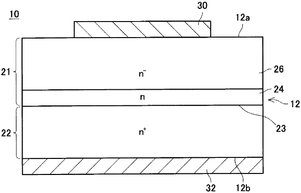
1. A semiconductor device comprising:
a first semiconductor layer having an N conductive type and made of a gallium oxide-based semiconductor; and
a second semiconductor layer made of a gallium oxide-based semiconductor, in contact with the first semiconductor layer, and having the N conductive type with an electrically active donor concentration higher than an electrically active donor concentration of the first semiconductor layer, wherein:
a difference between a donor concentration of the first semiconductor layer and a donor concentration of the second semiconductor layer is smaller than a difference between the electrically active donor concentration of the first semiconductor layer and the electrically active donor concentration of the second semiconductor layer,
the first semiconductor layer includes:
a transition layer in contact with the second semiconductor layer; and
a drift layer in contact with the transition layer and separated from the second semiconductor layer by the transition layer;
the electrically active donor concentration of the second semiconductor layer is 1×10¹⁸/cm3 or more;
the electrically active donor concentration in the transition layer is less than 1×10¹⁸/cm3;
the electrically active donor concentration of the drift layer is less than the electrically active donor concentration of the transition layer;
the electrically active donor concentration in the transition layer is distributed to decrease from the second semiconductor layer toward the drift layer;
in a stacking direction of the second semiconductor layer, the transition layer, and the drift layer, a rate of change in the electrically active donor concentration in the transition layer is 1×10¹⁵/cm3 or more per 1 μm;
in the stacking direction, the rate of change of the electrically active donor concentration in the drift layer is less than 1×10¹⁵/cm3 per 1 μm; and
a thickness of the transition layer is 0.1 μm or more.
|