| CPC H01L 29/167 (2013.01) [B82Y 10/00 (2013.01); H01L 21/823821 (2013.01); H01L 27/0886 (2013.01); H01L 27/0924 (2013.01); H01L 29/0847 (2013.01); H01L 29/161 (2013.01); H01L 29/41725 (2013.01); H01L 29/42392 (2013.01); H01L 29/66 (2013.01); H01L 29/66356 (2013.01); H01L 29/66439 (2013.01); H01L 29/66795 (2013.01); H01L 29/7391 (2013.01); H01L 29/775 (2013.01); H01L 29/785 (2013.01); H01L 29/7851 (2013.01); H01L 29/78618 (2013.01); H01L 29/78696 (2013.01); H01L 29/0834 (2013.01); H01L 29/66545 (2013.01)] | 16 Claims |

|
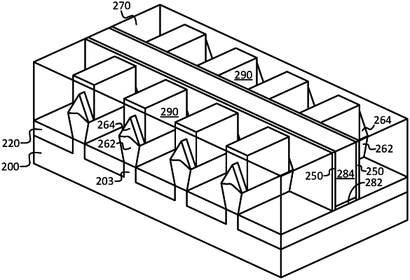
1. An integrated circuit (IC) comprising:
a transistor including
a gate structure;
a semiconductor region below the gate structure, the semiconductor region including a first group IV semiconductor material;
a p-type source region and an n-type drain region adjacent to the semiconductor region, the p-type source and n-type drain regions including a second group IV semiconductor material that is different from the first group IV semiconductor material, wherein at least one of the p-t pe source or n-type drain regions includes two or more of sulfur (S), selenium (Se), or tellurium (Te) combined with a single-charge dopant species selected from the group consisting of P, As and B, and the other of the p-type source or n-type drain regions does not include double-charge dopants; and
a source contact structure and a drain contact structure connected to the p-type source region and the n-type drain region, respectively.
|