| CPC H01L 29/105 (2013.01) [H01L 29/41775 (2013.01); H01L 29/41783 (2013.01); H01L 29/6656 (2013.01); H01L 29/66545 (2013.01); H01L 29/66628 (2013.01); H01L 29/7834 (2013.01); H01L 29/165 (2013.01); H01L 29/665 (2013.01); H01L 29/7848 (2013.01)] | 16 Claims |
|
1. A method for forming a field effect transistor (FET), comprising:
choosing a semiconductor substrate for the FET from a group comprising a silicon wafer, a partially depleted silicon on insulator (PDSOI), and fully depleted silicon on insulator (FDSOI), the semiconductor substrate having a planar surface and a semiconductor body within the semiconductor substrate below the planar surface;
defining an active area using a shallow trench isolation, within the semiconductor substrate and on the planar surface of the semiconductor substrate for the FET, wherein the active area is isolated within the shallow trench isolation;
doping the active area, using a dopant of a first type, chosen from one of a p-type dopant or a n-type dopant, the n-type and p-type being opposite dopant types from each other;
growing or depositing, on the planar surface over the active area, one or more layers as a gate dielectric having a thickness and a composition suitably chosen to handle an operating voltage of the FET;
depositing one or more layers of a conductive gate electrode material over the gate dielectric;
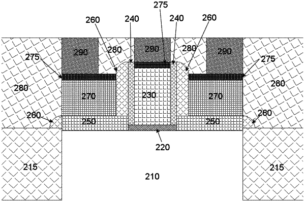
masking and selectively removing the conductive gate electrode material and the gate dielectric to form a conductive gate electrode and to divide the active area into three regions along a direction of carrier flow in the FET, the three regions comprising a source extension area, a gate region and a drain extension area, wherein the gate region separates the source extension area and drain extension area, which are on opposite sides of the gate region;
depositing a gate side wall dielectric of a thickness suitably chosen to handle the operating voltage conditions of the FET to cover the sides of the gate electrode, the gate side wall dielectric having a thickness similar to the thickness of the gate dielectric;
selectively removing any of the deposited gate side wall dielectric from the source extension area and the drain extension area using anisotropic etching to expose the planar surface of the doped semiconductor substrate while retaining the gate side wall dielectric as protection for the conductive gate electrode;
depositing, using selective epitaxial growth at a temperature in the range of 500° C. to 700° C., a source extension epitaxial layer and a drain extension epitaxial layer, the source and drain extension epitaxial layers having a thickness in the range of 3 to 20 nm, wherein the source and drain extension epitaxial layers are doped during deposition using a dopant of a second type opposite to the first type, the source extension epitaxial layer being grown selectively over and in contact with the source extension area of the exposed planar surface of the semiconductor active area and the drain extension epitaxial layer being grown selectively over and in contact with the drain extension area of the exposed planar surface of the semiconductor active area, the drain extension epitaxial layer and source extension epitaxial layer being adjacent the gate side wall dielectric on opposite sides of the conductive gate electrode, but isolated from the conductive gate electrode by the gate side wall dielectric;
forming spacers by conformally depositing a spacer dielectric having a spacer thickness, and anisotropically etching the spacer dielectric to expose a top surface of the source extension epitaxial layer and a top surface of the drain extension epitaxial layer while leaving the spacers over the gate side wall dielectric, the bottom of the spacers terminating on the top surface of the source extension epitaxial layer and on the top surface of the drain extension epitaxial layer, and respectively covering the source and drain extension epitaxial layers to a spacer distance from the gate side wall dielectric; and
growing at least one additional doped epitaxial layer on the exposed top surface of source and drain extension epitaxial layers using selective epitaxial growth at a temperature in the range of 500° C. to 700° C. to create a source epitaxial layer over the exposed top surface of the source extension epitaxial layer and a drain epitaxial layer over the exposed top surface of the drain extension epitaxial layer, the at least one additional doped epitaxial layer being doped during deposition using the dopant of the second type to a higher doping concentration than that of the source extension epitaxial layer;
wherein a source of the FET comprises the source extension epitaxial layer contacting the planar surface of the semiconductor substrate, with the source epitaxial layer being in contact with and on the source extension epitaxial layer, and wherein a drain of the FET comprises the drain extension epitaxial layer contacting the planar surface of the semiconductor substrate, with the drain epitaxial layer being in contact with and on the drain extension epitaxial layer;
wherein the deposited source extension and drain extension and the gate are coplanar on the surface of the semiconductor surface, and the source extension and drain extension are separated from the gate electrode on the surface of the semiconductor surface by the deposited gate side wall dielectric on the gate electrode.
|