| CPC H01L 29/0847 (2013.01) [H01L 29/0634 (2013.01); H01L 29/1095 (2013.01); H01L 29/4236 (2013.01); H01L 29/66666 (2013.01); H01L 29/7827 (2013.01); H01L 21/26513 (2013.01)] | 24 Claims |
|
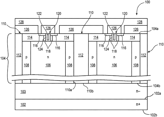
1. A method of making a semiconductor device, comprising:
providing a substrate;
disposing a semiconductor layer over the substrate;
forming a first trench through the semiconductor layer;
forming a second trench through the semiconductor layer;
forming a plug region in the semiconductor layer extending between the first trench and second trench;
forming a body region within the plug region;
forming a source/drain region extending across a portion of the plug region and further extending across a portion of the body region;
forming a gate trench adjacent to the source/drain region and extending through the body region to the semiconductor layer;
disposing a dielectric layer within the gate trench; and
disposing a trench gate electrode within the gate trench.
|