| CPC H01L 29/0684 (2013.01) [H01L 21/02543 (2013.01); H01L 21/02546 (2013.01); H01L 29/0669 (2013.01); H01L 29/0847 (2013.01); H01L 29/1033 (2013.01); H01L 29/205 (2013.01); H01L 29/41758 (2013.01); H01L 29/66522 (2013.01); H01L 29/66795 (2013.01); H01L 29/7851 (2013.01)] | 20 Claims |
|
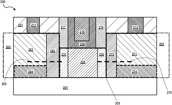
1. A semiconductor device, comprising:
a nanowire including a channel compound semiconductor material; and
a source area including a first portion and a second portion of the source area, wherein an interface between the nanowire and the source area includes the channel compound semiconductor material, the second portion of the source area is adjacent to the interface between the nanowire and the source area, the first portion of the source area is separated from the interface between the nanowire and the source area by the second portion of the source area, the first portion of the source area includes a first compound semiconductor material, and the second portion of the source area includes a second compound semiconductor material, and wherein the channel compound semiconductor material has a channel material bandgap and a lattice constant, the first compound semiconductor material has a first bandgap and the lattice constant, the second compound semiconductor material has a second bandgap and the lattice constant.
|