| CPC H01L 29/0673 (2013.01) [H01L 21/02381 (2013.01); H01L 21/02433 (2013.01); H01L 29/42392 (2013.01); H01L 29/6656 (2013.01); H01L 29/66545 (2013.01); H01L 29/66795 (2013.01); H01L 29/785 (2013.01); H01L 2029/7858 (2013.01)] | 20 Claims |
|
1. A semiconductor device, comprising:
a substrate comprising a semiconductor material with a predetermined crystal orientation;
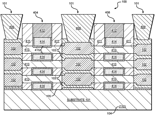
a gate stack comprising a plurality of nanosheet channel layers, each nanosheet channel layer being controlled by metal gate electrodes located above and below the nanosheet channel layer, each nanosheet channel layer comprising the same semiconductor material and crystal orientation as that of the substrate;
a source/drain region including a source/drain epitaxy on each of opposite sides of the gate stack, each source/drain region comprising a plurality of separated bridging structures respectively connected to each nanosheet channel layer;
a metal wrap-around-contact separately located in each source/drain region, the metal wrap-around-contact located in spaces between the bridging structures and encapsulating the bridging structures,
wherein the bridging structures are entirely embedded in the metal wrap-around-contact, and the bridging structures are each separated from each other,
wherein the source/drain epitaxy includes a crystal structure Si (100) that is a single merged epitaxy component.
|