|
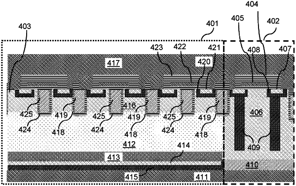
1. An apparatus, comprising: an insulated gate bipolar transistor (GBT) having a gate comprising a gate insulating layer formed on top of a first shield electrode extending into a drift region of a first conductivity type, the insulated gate bipolar transistor further having an implanted layer of a second conductivity type opposite the first conductivity type, a buffer layer of the first conductivity type between the drift region and the implanted region and a lightly doped layer of either the first conductivity type or the second conductivity type between the buffer region and the implanted region; and a super-junction metal-oxide semiconductor field effect transistor (SJ-MOSFET) having a drift region of the first conductivity type, a heavily doped bottom layer of a first conductivity type, wherein the drift region is of the first conductivity type, wherein the IGBT and the SJ-MOSFET are structurally coupled by a common substrate, wherein an emitter of the insulated gate bipolar transistor and a source of the super-junction metal-oxide semiconductor field effect transistor are conductively coupled by a contact metal, wherein a collector of the insulated gate bipolar transistor and a drain of the super-junction metal-oxide semiconductor field effect transistor are conductively coupled by a backside contact.
|
