| CPC H01L 27/156 (2013.01) | 20 Claims |
|
1. A light source comprising:
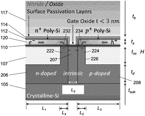
a structure comprising indirect bandgap semiconductor material formed on a substrate, the structure having a maximum dimension that is no larger than 1000 nm and a minimum dimension that is no smaller than 25 nm and wherein the structure includes a semiconductor junction and a radiative recombination region formed from the indirect bandgap semiconductor material;
a first region of n-type semiconductor material connected to the structure and arranged to inject electrons into the radiative recombination region in a first direction; and
a second region of p-type semiconductor material connected to the structure and arranged to inject holes into the radiative recombination region in a second direction such that the electrons and the holes recombine in the radiative recombination region to produce photons, wherein the electrons and the holes are injected into the structure across an oxide barrier when the light source is operating.
|