| CPC H01L 27/14652 (2013.01) [H01L 27/1462 (2013.01); H01L 27/14605 (2013.01)] | 20 Claims |

|
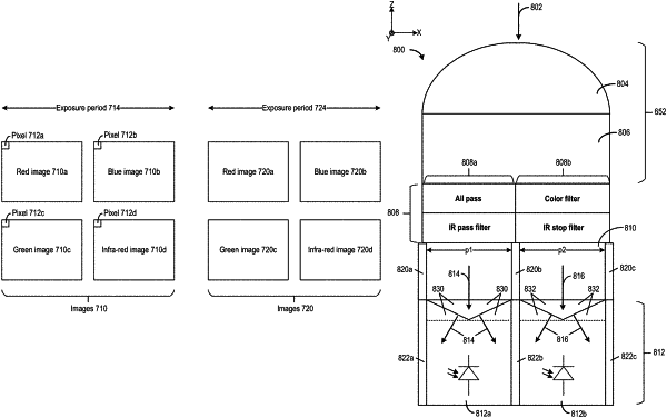
1. An apparatus, comprising:
a semiconductor substrate including a first photodiode and a second photodiode, the first photodiode being positioned adjacent to the second photodiode along a first axis, the first photodiode being configured to convert a first component of light to a first charge, the second photodiode being configured to convert a second component of the light to a second charge, the first component and the second component being associated with, respectively, a first wavelength and a second wavelength;
a first optical structure and a second optical structure positioned over, respectively, the first photodiode and the second photodiode along a second axis perpendicular to the first axis,
wherein:
the first optical structure is configured to:
receive the first component of the light at a first angle with respect to the second axis, and
steer the first component of the light at a second angle with respect to the second axis towards the first photodiode, the second angle being configured to increase a propagation path of the first component of the light within the first photodiode compared with the first angle;
the second optical structure is configured to:
receive the second component of the light at a third angle with respect to the second axis, and
steer the second component of the light at a fourth angle with respect to the second axis towards the second photodiode, the fourth angle being configured to increase a propagation path of the second component of the light within the second photodiode compared with the third angle;
the first optical structure has a first optical property based on the first wavelength; and
the second optical structure has a second optical property based on the second wavelength; and
an optical element positioned over the first optical structure and the second optical structure along the second axis to receive the light and to project the light towards the first optical structure and the second optical structure.
|
|
17. An apparatus comprising:
an array of pixel cells, each pixel cell comprising:
a semiconductor substrate including a first photodiode and a second photodiode, the first photodiode being positioned adjacent to the second photodiode along a first axis, the first photodiode being configured to convert a first component of light to a first charge, the second photodiode being configured to convert a second component of the light to a second charge, the first component and the second component being associated with, respectively, a first wavelength and a second wavelength; and
a first optical structure and a second optical structure positioned over, respectively, the first photodiode and the second photodiode along a second axis perpendicular to the first axis,
wherein:
the first optical structure is configured to:
receive the first component of the light at a first angle with respect to the second axis, and
steer the first component of the light at a second angle with respect to the second axis towards the first photodiode, the second angle being configured to increase a propagation path of the first component of the light within the first photodiode compared with the first angle;
the second optical structure is configured to:
receive the second component of the light at a third angle with respect to the second axis, and
steer the second component of the light at a fourth angle with respect to the second axis towards the second photodiode, the fourth angle being configured to increase a propagation path of the second component of the light within the second photodiode compared with the third angle;
the first optical structure has a first optical property based on the first wavelength; and
the second optical structure has a second optical property based on the second wavelength;
and
one or more optical elements positioned over the array of pixel cells along the second axis to receive the light and to project the light towards the first optical structure and the second optical structure of each pixel cell of the array of pixel cells.
|