| CPC H01L 27/14605 (2013.01) [H01L 27/1463 (2013.01); H01L 27/1465 (2013.01); H01L 27/1469 (2013.01); H01L 27/14621 (2013.01); H01L 27/14627 (2013.01); H01L 27/14632 (2013.01); H01L 27/14634 (2013.01); H01L 27/14636 (2013.01); H01L 27/14645 (2013.01); H01L 27/14649 (2013.01); H01L 27/14685 (2013.01); H01L 27/14687 (2013.01); H01L 27/14689 (2013.01); H01L 27/14698 (2013.01); H01L 31/02327 (2013.01); H01L 31/0312 (2013.01); H01L 31/09 (2013.01); H01L 31/105 (2013.01); H01L 31/1812 (2013.01); H01L 31/1876 (2013.01); H01L 31/1892 (2013.01)] | 13 Claims |
|
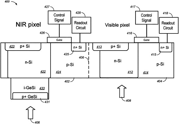
1. An image sensor comprising:
an absorption region configured to absorb photons having a wavelength within an infrared wavelength range or a near-infrared wavelength range, and to generate photo-carriers from the absorbed photons within the infrared or near-infrared wavelength ranges;
a first n-doped silicon region in contact with the absorption region;
a first p-doped silicon region in contact with the first n-doped silicon region;
a second n-doped silicon region in contact with the first p-doped silicon region and electrically coupled to a readout circuitry; and
a second p-doped silicon region, wherein a surface of the second p-doped silicon region is coplanar with a surface of the first n-doped silicon region, and wherein the second p-doped silicon region is more heavily doped than the first p-doped silicon region,
wherein the absorption region comprises a first surface and a second surface, wherein the first surface is in contact with the first n-doped silicon region, wherein the second surface is opposite to the first surface, and
wherein the absorption region comprises a p-doped absorption region adjacent to the second surface, the p-doped absorption region comprising germanium.
|