| CPC H01L 27/1255 (2013.01) [G02F 1/1368 (2013.01); G02F 1/136209 (2013.01); G02F 1/136213 (2013.01); G03B 21/2013 (2013.01); H01L 27/1248 (2013.01)] | 8 Claims |
|
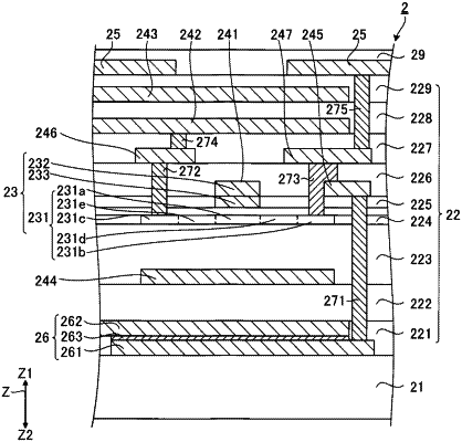
1. An electro-optical device comprising:
a substrate having light-transmissivity,
a transistor having a semiconductor layer,
a capacitance element having light-transmissivity and including a first electrode, a dielectric layer, and a second electrode, the capacitance element being disposed between the substrate and the transistor in a thickness direction of the substrate,
a light-shielding film disposed between the capacitance element and the transistor in the thickness direction of the substrate,
a first insulating film having light-transmissivity, and disposed between the light-shielding film and the capacitance element in the thickness direction of the substrate,
a second insulating film having light-transmissivity, and disposed between the first insulating film and the semiconductor layer, and
a third insulating film having light-transmissivity, and disposed between the first insulating film and the substrate in the thickness direction of the substrate, wherein
an entirety of the capacitance element is disposed in the third insulating film, and
each refractive index of the first electrode, the second electrode, and light-shielding film is higher than each refractive index of the dielectric layer, the first insulating film, and the second insulating film.
|