| CPC H01L 27/0922 (2013.01) [H01L 21/02532 (2013.01); H01L 21/02603 (2013.01); H01L 21/28088 (2013.01); H01L 21/28158 (2013.01); H01L 21/3115 (2013.01); H01L 21/31111 (2013.01); H01L 21/31144 (2013.01); H01L 21/823807 (2013.01); H01L 21/823842 (2013.01); H01L 21/823857 (2013.01); H01L 29/0673 (2013.01); H01L 29/408 (2013.01); H01L 29/42392 (2013.01); H01L 29/4908 (2013.01); H01L 29/66545 (2013.01); H01L 29/78618 (2013.01); H01L 29/78696 (2013.01); H01L 2029/42388 (2013.01)] | 20 Claims |
|
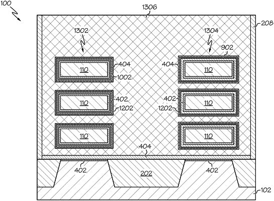
1. A semiconductor device comprising at least:
a first transistor having a first threshold voltage, the first transistor comprising at least
a first gate structure surrounding one or more nanosheet channel layers of the first
transistor, wherein the first gate structure comprises a first dielectric layer comprising a first thickness; and
a second transistor having a second threshold voltage that is different than the first threshold voltage, the second transistor comprising at least
a second gate structure surrounding one or more nanosheet channel layers of the
second transistor, wherein the second gate structure comprises a second dielectric layer comprising a second thickness that is greater than the first thickness.
|