| CPC H01L 25/18 (2013.01) [G06F 3/0604 (2013.01); G06F 3/0659 (2013.01); G06F 3/0679 (2013.01); G11C 16/10 (2013.01); G11C 16/26 (2013.01); G11C 16/30 (2013.01); H01L 24/13 (2013.01); H01L 24/16 (2013.01); H01L 24/48 (2013.01); H01L 24/73 (2013.01); G11C 16/0483 (2013.01); H01L 2224/13016 (2013.01); H01L 2224/16057 (2013.01); H01L 2224/16145 (2013.01); H01L 2224/48106 (2013.01); H01L 2224/48145 (2013.01); H01L 2224/73207 (2013.01)] | 20 Claims |
|
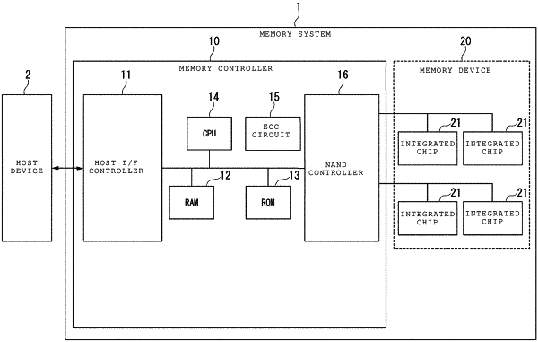
1. A semiconductor storage device, comprising:
a plurality of memory chips, each of which has a memory cell array including a plurality of memory cells; and
a circuit chip including:
a data latch configured to store data in unit of page data, for writing data into or reading data from the memory cell array of each of the memory chips;
a first power line connected to the circuit chip via a first bonding wire;
a first signal line connected to the circuit chip via a second bonding wire;
a second power line connected between the circuit chip and one of the memory chips via a first micro bump; and
a second signal line connected between the circuit chip and one of the memory chips via a second micro bump,
the plurality of memory chips and the circuit chip being stacked on each other in a stacking direction.
|