| CPC H01L 25/0655 (2013.01) [H01L 21/56 (2013.01); H01L 23/3121 (2013.01); H01L 23/5386 (2013.01); H01L 23/642 (2013.01); H01L 24/13 (2013.01); H01L 25/50 (2013.01); H01L 2224/13147 (2013.01)] | 11 Claims |
|
1. A method comprising:
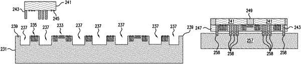
providing a spacer wafer, said spacer wafer having inner and outer surfaces, said spacer wafer including at least first and second semiconductor circuit features and wiring, adjacent said outer surface;
forming a plurality of trenches partially through said spacer wafer, spaced from said at least first and second semiconductor circuit features and said wiring;
providing first and second semiconductor dies, each having a plurality of electrical interconnect pillars and a plurality of contact pads, said electrical interconnect pillars having distal ends;
securing said first and second semiconductor dies to said spacer wafer via said plurality of contact pads with said interconnect pillars extending into said trenches, and with said contact pads coupled to said wiring and said semiconductor circuit features, to form a spacer-chip assembly;
processing said inner surface of said of said spacer wafer to open said trenches and expose said distal ends of said pillars;
applying electrically conductive connective material to said distal ends of said pillars; and
securing said spacer-chip assembly to a substrate via said electrically conductive connective material on said distal ends of said pillars.
|