| CPC H01L 25/0652 (2013.01) [H01L 2225/0652 (2013.01); H01L 2225/06506 (2013.01); H01L 2225/06513 (2013.01); H01L 2225/06517 (2013.01); H01L 2225/06527 (2013.01)] | 15 Claims |
|
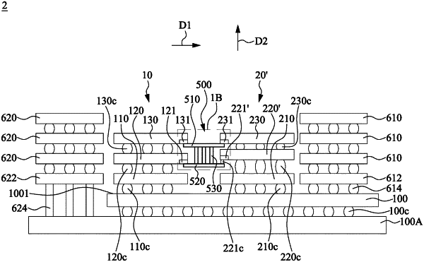
1. A semiconductor package structure, comprising:
a carrier;
a first electronic component disposed over a surface of the carrier;
a second electronic component disposed over the first electronic component;
a third electronic component spaced apart from the first electronic component and disposed over the surface of the carrier;
a fourth electronic component disposed over the third electronic component; and
a connection element electrically connecting the second electronic component to the fourth electronic component, the connection element being external to the carrier,
wherein the connection element is configured to control transmission paths between the first electronic component, the second electronic component, the third electronic component, and the fourth electronic component; and
wherein the connection element is configured to adjust bandwidths of the transmission paths between the first electronic component, the second electronic component, the third electronic component, and the fourth electronic component.
|