| CPC H01L 24/46 (2013.01) [H01L 24/06 (2013.01); H01L 25/0657 (2013.01); H01L 2224/06515 (2013.01); H01L 2224/46 (2013.01); H01L 2225/0651 (2013.01); H01L 2225/06506 (2013.01); H01L 2225/06562 (2013.01); H01L 2924/1435 (2013.01)] | 20 Claims |
|
1. A semiconductor device, comprising:
a first terminal on a substrate;
a second terminal on the substrate;
a plurality of third terminals on the substrate;
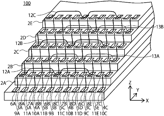
a plurality of memory chips stacked on the substrate in an offset manner, each memory chip including first pads, second pads, and third pads;
a first bonding wire that is electrically connected to the first terminal and physically connected to a first pad of different memory chips in the plurality;
a second bonding wire that is electrically connected to the second terminal and physically connected to a second pad of the different memory chips;
a third bonding wire that electrically connects one third terminal to a third pad of the different memory chips; and
a fourth bonding wire connected to the first bonding wire at a first pad on a first memory chip in the plurality and another first pad on the first memory chip, the fourth bonding wire straddling over the second bonding wire connected to a second pad on the first memory chip and the third bonding wire connected to a third pad on the first memory chip.
|