| CPC H01L 24/09 (2013.01) [H01L 24/49 (2013.01); H01L 25/072 (2013.01); H01L 22/14 (2013.01); H01L 22/30 (2013.01); H01L 22/32 (2013.01); H01L 23/49541 (2013.01); H01L 23/49548 (2013.01); H01L 23/49558 (2013.01); H01L 23/49562 (2013.01); H01L 23/49575 (2013.01); H01L 2224/04042 (2013.01); H01L 2924/13055 (2013.01); H01L 2924/13091 (2013.01); H01L 2924/30101 (2013.01)] | 20 Claims |

|
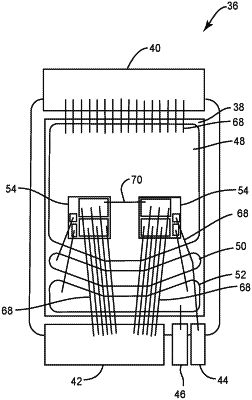
1. A package for power electronics comprising:
a power substrate;
a power switching conductive trace on the power substrate;
at least one power semiconductor die on the power switching conductive trace, the at least one power semiconductor die comprising:
a first power switching pad and a second power switching pad;
a control pad;
a semiconductor structure configured such that a resistance of a power switching path between the first power switching pad and the second power switching pad is based on a control signal provided at the control pad; and
a Kelvin connection pad coupled to the second power switching pad on the at least one power semiconductor die;
a Kelvin conductive trace on the power substrate;
a Kelvin connection contact coupled to the Kelvin connection pad via the Kelvin conductive trace; and
a control conductive trace coupled to the control pad, wherein the control conductive trace is arranged on the power substrate and between the power switching conductive trace and the Kelvin conductive trace.
|