| CPC H01L 24/08 (2013.01) [H01L 24/80 (2013.01); H01L 25/0657 (2013.01); H01L 25/18 (2013.01); H01L 25/50 (2013.01); H01L 2224/08145 (2013.01); H01L 2224/80895 (2013.01); H01L 2224/80896 (2013.01); H01L 2924/1431 (2013.01); H01L 2924/14511 (2013.01)] | 20 Claims |
|
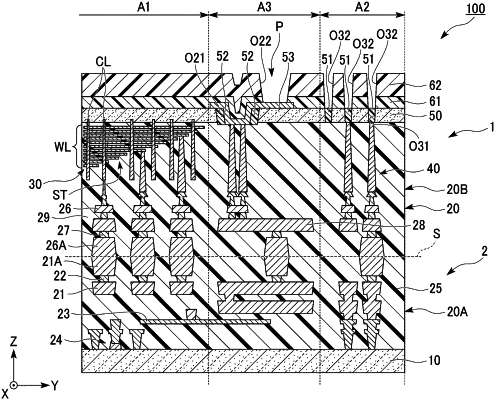
1. A semiconductor storage device comprising:
a first chip including a first substrate, a transistor, and a first pad, the transistor being on the first substrate, the first pad being above the transistor; and
a second chip including a second pad, a memory cell array, and a second substrate, the second pad being on the first pad, the memory cell array being above the second pad and including a plurality of memory cells, the second substrate being above the memory cell array, the second chip being bonded to the first chip,
wherein
the first chip and the second chip includes, when viewed in a first direction orthogonal to the first substrate, a first region and a second region, the first region including the memory cell array, the second region surrounding an area around the first region and including a wall extending from the first substrate to the second substrate, and
the second substrate includes a first opening passing through the second substrate in the second region.
|