| CPC H01L 23/66 (2013.01) [H01L 21/486 (2013.01); H01L 21/4857 (2013.01); H01L 21/56 (2013.01); H01L 23/295 (2013.01); H01L 23/315 (2013.01); H01L 23/367 (2013.01); H01L 23/49816 (2013.01); H01L 23/49822 (2013.01); H01L 23/49844 (2013.01); H01L 23/5383 (2013.01); H01L 23/5386 (2013.01); H01L 24/16 (2013.01); H01L 24/24 (2013.01); H01L 25/165 (2013.01); H01L 2223/6616 (2013.01); H01L 2224/16238 (2013.01); H01L 2224/24137 (2013.01); H01L 2924/1205 (2013.01); H01L 2924/1206 (2013.01); H01L 2924/14215 (2013.01)] | 20 Claims |
|
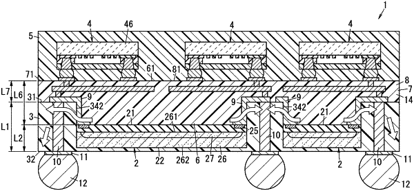
1. An electronic module comprising:
a semiconductor element;
a first insulating layer covering at least an outer peripheral surface of the semiconductor element and including a first principal surface and a second principal surface that face each other;
an electronic element electrically connected to the semiconductor element and having electrical characteristics;
a second insulating layer covering at least an outer peripheral surface of the electronic element;
at least a portion of the electronic element and at least a portion of the semiconductor element overlapping each other in plan view in a thickness direction of the first insulating layer;
a first intermediate layer interposed between the electronic element and the semiconductor element and having a thermal conductivity lower than a thermal conductivity of the first insulating layer and a thermal conductivity of the second insulating layer; and
a second intermediate layer interposed between the first insulating layer and the second insulating layer and having a thermal conductivity lower than the thermal conductivity of the first insulating layer and the thermal conductivity of the second insulating layer; wherein
a step is provided between the first principal surface of the first insulating layer, which is in contact with the second intermediate layer, and one principal surface of the semiconductor element, which is in contact with the first intermediate layer, and a distance between the second principal surface and the first principal surface of the first insulating layer is greater, in the thickness direction, than a distance between the second principal surface of the first insulating layer and the one principal surface of the semiconductor element.
|