| CPC H01L 23/66 (2013.01) [H01L 23/49838 (2013.01); H01L 24/81 (2013.01); H03H 11/28 (2013.01); H03M 9/00 (2013.01); H01L 2223/6616 (2013.01); H01L 2224/81908 (2013.01); H01L 2224/81986 (2013.01); H01L 2924/30105 (2013.01); H01L 2924/30111 (2013.01)] | 14 Claims |
|
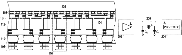
1. A method of providing a connection from an integrated circuit signal pad to a printed circuit board trace, the method comprising:
obtaining an expected impedance of the PCB trace;
determining a first parasitic capacitance of a core via;
estimating a second parasitic capacitance of a solder ball connection between a package substrate pad and the PCB trace;
calculating a pi-network inductance that, together with the first and second parasitic capacitances, provides impedance matching with the expected impedance of the PCB trace; and
adjusting a micro-via arrangement between the core via and the solder ball connection to provide the pi-network inductance, the micro-via arrangement including at least a first, second, and third micro-vias, wherein said adjusting includes:
offsetting the second micro-via in a first direction from the first micro-via; and
offsetting the third micro-via from the second micro-via in a direction perpendicular to the first direction.
|