| CPC H01L 23/66 (2013.01) [H01Q 1/2283 (2013.01); H01L 2223/6616 (2013.01); H01L 2223/6677 (2013.01)] | 20 Claims |
|
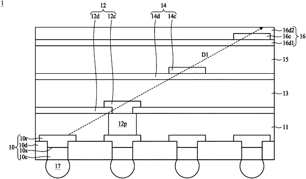
1. A semiconductor device package, comprising:
a substrate having an upper surface;
a reflector disposed above the upper surface of the substrate;
a radiator disposed above the reflector; and
a first director disposed above the radiator,
wherein the reflector, the radiator, and the first director collectively define an antenna, the reflector, the radiator, and the first director are free from overlapping each other vertically from a cross-sectional view perspective, and a radiation direction of the antenna is non-parallel to the upper surface of the substrate.
|