| CPC H01L 23/66 (2013.01) [H01Q 1/48 (2013.01); H01Q 1/526 (2013.01); H01Q 5/378 (2015.01); H01Q 13/08 (2013.01); H01Q 13/10 (2013.01); H01Q 23/00 (2013.01); H01L 2223/6677 (2013.01)] | 12 Claims |
|
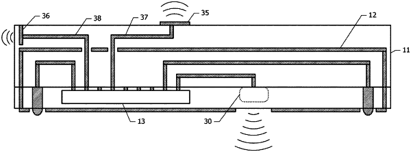
1. A high-frequency module comprising:
a dielectric substrate;
a ground plane provided in the dielectric substrate or on a top surface of the dielectric substrate;
a high-frequency semiconductor device mounted on a bottom surface of the dielectric substrate;
a shield structure provided in a space closer to the bottom surface than the ground plane is and surrounding the high-frequency semiconductor device from below and from side of the high-frequency semiconductor device, the shield structure being connected to the ground plane and having an opening;
a radiation-structure portion for radiating a high-frequency signal outputted by the high-frequency semiconductor device as electromagnetic waves through the opening; and
an upper radiating element provided at a portion of the dielectric substrate above the ground plane and driven by the high-frequency semiconductor device.
|