| CPC H01L 23/552 (2013.01) [H01L 21/56 (2013.01); H01L 23/5389 (2013.01); H01L 24/32 (2013.01); H01L 2224/32227 (2013.01)] | 15 Claims |
|
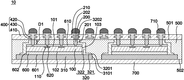
1. A semiconductor package structure, comprising:
an electronic component having a first surface, a lateral surface adjacent to the first surface, and a second surface opposite to the first surface;
a conductive contact connected to the first surface of the electronic component;
a first shielding layer disposed on the lateral surface of the electronic component and a portion of the first surface of the electronic component, the first shielding layer contacting the conductive contact; and
an encapsulant encapsulating the electronic component, the conductive contact, and the first shielding layer;
wherein a surface of the encapsulant and a surface of the conductive contact are substantially coplanar.
|