| CPC H01L 23/5381 (2013.01) [H01L 21/486 (2013.01); H01L 21/4853 (2013.01); H01L 21/565 (2013.01); H01L 21/6835 (2013.01); H01L 23/3107 (2013.01); H01L 23/5384 (2013.01); H01L 23/5386 (2013.01); H01L 23/562 (2013.01); H01L 25/0652 (2013.01); H01L 25/50 (2013.01); H01L 2221/68372 (2013.01); H01L 2225/06513 (2013.01); H01L 2225/06548 (2013.01); H01L 2225/06558 (2013.01); H01L 2225/06582 (2013.01); H01L 2225/06589 (2013.01)] | 20 Claims |
|
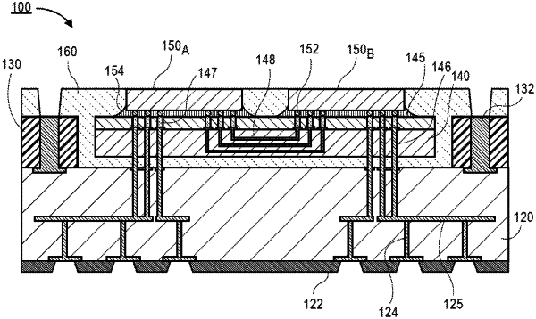
1. An electronic device package, comprising:
a bridge die having a top, a bottom, a first side between the top and bottom, and a second side between the top and bottom, the second side opposite the first side, the bridge die having a vertical thickness between the top and bottom;
an encapsulation layer laterally adjacent to and in contact with the first side and the second side of the bridge die;
a first conductive via laterally adjacent to the first side of the bridge die, wherein a first portion of the encapsulation layer is between the first conductive via and the first side of the bridge die, wherein the first conductive via has a vertical thickness greater than the vertical thickness of the bridge die, and wherein the vertical thickness of the first conductive via extends along an entirety of the vertical thickness of the bridge die to a first location below the bottom of the bridge die;
a second conductive via laterally adjacent to the second side of the bridge die, wherein a second portion of the encapsulation layer is between the second conductive via and the second side of the bridge die, wherein the second conductive via has a vertical thickness greater than the vertical thickness of the bridge die, and wherein the vertical thickness of the second conductive via extends along an entirety of the vertical thickness of the bridge die to a second location below the bottom of the bridge die;
a first die coupled to the bridge die; and
a second die coupled to the bridge die, the second die electrically coupled to the first die by electrical traces in the bridge die.
|