| CPC H01L 23/5226 (2013.01) [H01L 23/298 (2013.01); H01L 23/3178 (2013.01); H01L 24/20 (2013.01)] | 28 Claims |
|
1. A method of manufacturing a device, the method comprising:
forming a cavity in a substrate extending at least partially through a thickness of the substrate from a surface of the substrate;
providing a conductive material in the cavity and over the surface of the substrate;
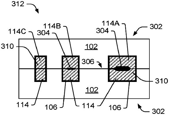
removing a portion of the conductive material thereby forming a recess on an upper surface of the conductive material;
providing a fill layer over the upper surface of the conductive material and the surface of the substrate;
removing at least a portion of the fill layer to expose at least a portion of the conductive material; and
forming a second cavity in the substrate extending at least partially though the thickness of the substrate from the surface of the substrate, a width of the second cavity being wider than a width of the cavity.
|