| CPC H01L 23/50 (2013.01) [H01L 23/315 (2013.01); H01L 23/3128 (2013.01)] | 21 Claims |
|
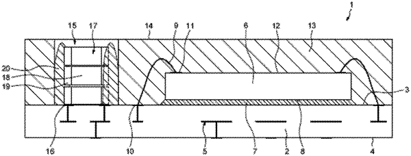
1. A process for producing an electronic device, comprising:
mounting an integrated circuit (IC) chip on top of a front face of a carrier substrate and connecting the IC chip to first electrical contacts of the front face of the carrier substrate;
forming an encapsulation block on top of the front face of the carrier substrate which embeds the IC chip;
making a through-void for positioning and confinement that extends through the encapsulation block, reaches the front face of the carrier substrate and exposes second electrical contacts of the front face of the carrier substrate;
placing a stack of electronic components in the through-void on top of the front face of the carrier substrate, wherein the through-void and the stack of electronic components are configured such that there is a clearance between flanks of the through-void and flanks of the stack of electronic components, and wherein an orientation of the stack of electronic components, parallel to the front face of the carrier substrate, is limited by at least two opposite flanks of the through-void;
dispensing solder material into the through-void such that the solder material penetrates into said clearance; and
hardening the solder material so that electrical connection terminals of each electronic component of the stack of electronic components are connected to the second electrical contacts of the front face of the carrier substrate by solder bumps or pads that are located in the through-void.
|