| CPC H01L 23/373 (2013.01) [H01L 23/3114 (2013.01); H01L 23/38 (2013.01); H01L 25/18 (2013.01); H01L 29/43 (2013.01); H10N 10/17 (2023.02)] | 14 Claims |
|
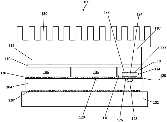
1. A microelectronic package structure comprising:
a substrate;
a first die on the substrate;
one or more additional dice on the first die;
a thermoelectric cooler (TEC) on the first die adjacent at least one of the one or more additional dice, wherein the TEC comprises a thermoelectric material, wherein a first side of the thermoelectric material is on the first die and wherein a dummy die is on a second side of the thermoelectric material, wherein the second side is opposite the first side; and
the dummy die on the TEC, wherein the dummy die is thermally coupled to the first die.
|