| CPC H01L 21/823487 (2013.01) [H01L 21/8221 (2013.01); H01L 21/823481 (2013.01); H01L 27/0688 (2013.01); H01L 29/66666 (2013.01); H01L 29/7827 (2013.01); H01L 29/41741 (2013.01)] | 20 Claims |
|
1. A method, comprising:
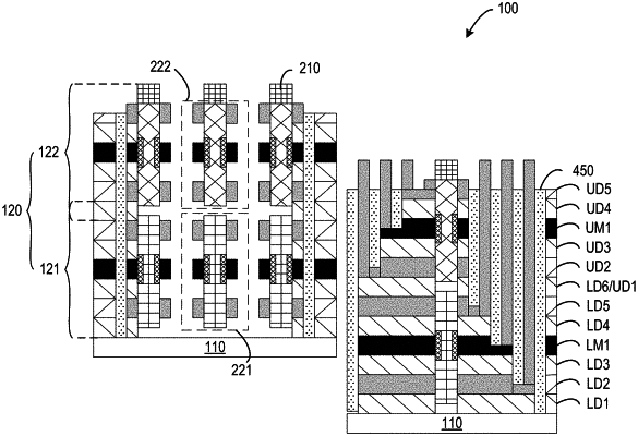
forming a layer stack on a substrate, the layer stack including alternating metal layers and dielectric layers;
forming vertically stacked lower and upper vertical channel structures that vertically extend through the layer stack, the lower and upper vertical channel structures being separated by a sacrificial layer;
forming source, drain and gate connections to the lower and upper vertical channel structures, the source, drain and gate connections extending horizontally from the lower and upper vertical channel structures and then vertically to a location above the upper vertical channel structure;
forming a vertical opening in the layer stack; and
removing the sacrificial layer through the vertical opening to separate the lower and upper vertical channel structures.
|