| CPC H01L 21/823481 (2013.01) [H01L 21/764 (2013.01); H01L 21/823431 (2013.01); H01L 27/0886 (2013.01)] | 20 Claims |
|
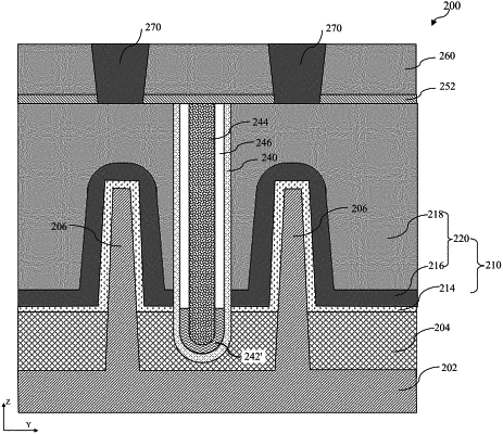
1. A method comprising:
forming a gate stack over a first fin and a second fin;
removing a portion of the gate stack to form a trench extending between a first remaining portion of the gate stack disposed over the first fin and a second remaining portion of the gate stack disposed over the second fin;
forming a first material layer in the trench;
forming a second material layer on the first material layer disposed in the trench;
forming a third material layer on the second material layer disposed in the trench;
removing a first portion of the second material layer to form a first air gap extending from a first edge of the first material layer to a first edge of the third material layer; and
forming a sealing layer over the first air gap.
|