| CPC H01L 21/76834 (2013.01) [H01L 21/28562 (2013.01); H01L 21/76832 (2013.01); H01L 23/5329 (2013.01)] | 13 Claims |
|
1. A method for a device structure for semiconductor devices, comprising:
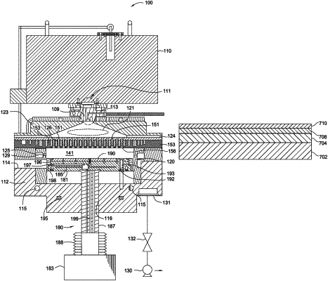
forming a film from a two-dimensional transition metal dichalcogenide and a process gas from a group consisting of 1,2-ethanedithiol, dimethyldisulfide, diethyldisulfide, and diethylsulfide, wherein the film is formed on a substrate in a first processing chamber disposed in a cluster processing system;
thermally treating the film to form a treated metal layer in a second processing chamber disposed in the cluster processing system, wherein the thermal treatment removes carbon from the film leaving only sulfur from the process gas and metal from a metal precursor to form a MX2 compound, wherein M comprises molybdenum (Mo) or tungsten (W) and X comprises sulfur (S); and
forming a capping layer on the MX2 compound in a third processing chamber disposed in the cluster processing system.
|