| CPC H01L 21/76802 (2013.01) [H01L 21/762 (2013.01); H01L 21/76808 (2013.01); H01L 21/76816 (2013.01); H01L 21/76877 (2013.01); H10B 43/20 (2023.02); H10B 43/35 (2023.02); H10B 43/40 (2023.02); H10B 43/50 (2023.02)] | 20 Claims |
|
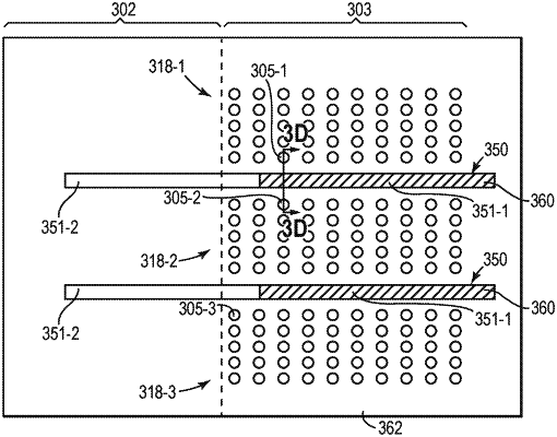
17. A method of forming a stacked memory array, comprising:
forming a stack of alternating first and second dielectrics;
forming an opening through the stack so that a first segment of the opening is between a first group of semiconductor structures and a second group of semiconductor structures in a first region of the stack and a second segment of the opening is in a second region of the stack that does not include the first and second semiconductor structures;
closing the first and second segments of the opening with a sacrificial material;
opening the closed second segment of the opening;
forming a third dielectric in the opened second segment of the opening; and
removing the sacrificial material from the closed first segment of the opening to form a new opening between the first group of semiconductor structures and the second group of semiconductor structures that terminates at the third dielectric.
|