| CPC H01L 21/485 (2013.01) [B29C 33/424 (2013.01); C25D 5/022 (2013.01); C25D 7/0678 (2013.01); C25D 17/001 (2013.01); H01L 21/6835 (2013.01); H01L 23/528 (2013.01); H05K 3/108 (2013.01); H05K 3/241 (2013.01); H01L 2221/1084 (2013.01); H01L 2221/68359 (2013.01); H01L 2224/95115 (2013.01); H05K 3/062 (2013.01)] | 17 Claims |
|
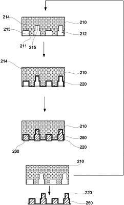
1. A method of forming a transferable metal interconnect layer (MIL), having a MIL design, for transferring to a device substrate, the method comprising:
depositing a seed layer on an engineered template, the engineered template comprising template features determined by the MIL design of the transferable MIL; and
selectively electroplating the transferable MIL into the template features over the seed layer,
wherein adhesion of the seed layer to the engineered template is below an adhesion threshold, corresponding to the device substrate, thereby allowing to transfer the transferable MIL from the engineered template to the device substrate while retaining the MIL design of the transferable MIL.
|