| CPC H01L 21/31155 (2013.01) [H01L 21/0234 (2013.01); H01L 21/02126 (2013.01); H01L 21/02216 (2013.01); H01L 21/02321 (2013.01); H01L 21/31116 (2013.01)] | 19 Claims |
|
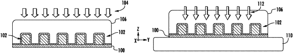
1. A method, comprising:
providing a substrate having a plurality of patterned features disposed directly on a first surface of the substrate, and a low dielectric constant layer disposed directly on and between the patterned features, the low dielectric constant layer characterized by a layer thickness;
heating the substrate to a substrate temperature in a range of 200° C. to 550° C.; and
directing an ion implant treatment to the low dielectric constant layer, while the substrate temperature is in the range of 200° C. to 550° C., wherein the ion implant treatment comprises:
implanting a low weight ion species, at an ion energy generating an implant depth equal to 40% to 175% of the layer thickness.
|